Conformal coating

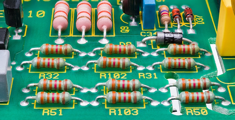
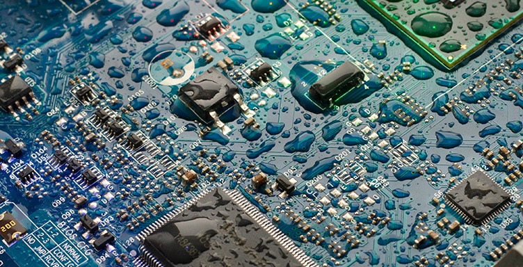
Conformal coating is utilized to safeguard the components on a printed circuit board against environmental factors such as moisture, dust, salt, and chemicals. To apply this coating, it’s crucial that the printed circuit board supports it.

Surface energy vs. surface tension

Surface chemistry is an extremely complex and challenging branch of science. You refer to surface energy in solids, while in liquids, you speak of surface tension. In practice, these terms are often used interchangeably.

Printed circuit boards & surface energy

The surface energy of solids is typically expressed in dynes per centimeter. We abbreviate this to ‘dynes’. The surface energy of a printed circuit board is generally determined by the solder mask. A common value is, for example, 36 dynes.

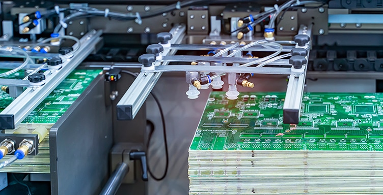
Inspection of printed circuit boards

To measure the surface energy of a printed circuit board, a line is often drawn on the board using a dyne pen. These pens contain a solution with a predetermined surface tension. If the surface energy needs to be 36 dynes, a corresponding pen is used to draw a line on a sample.

If this line forms a sharp edge without spreading on the print, the solder mask meets the specified surface energy.

How many dynes is sufficient?

It is important to discuss this with the supplier of the conformal coating. They know the required surface energy for the printed circuit board.

The Internet of Things

The Internet of Things enables “things” such as machines, sensors, or household appliances to communicate with each other and with humans. By adding sensors to these products, they can collect information and exchange it with other systems.

Possibilities

The Internet of Things creates new possibilities. This includes various sensors that help us improve the environment by continuously measuring air or water quality, or by tracking wildlife in their natural habitats. In the medical field, the Internet of Things is used for measuring blood pressure, pacemakers, or advanced hearing aids. Additionally, in industrial settings, existing products such as streetlights, bridges, and wind turbines are being equipped with smart sensors.

LoRa

LoRa stands for Long Range Radio and is a technology that enables data exchange over long distances without consuming much energy. As a result, some sensors can remain active for up to 15 years on a small energy source. LoRa is used for equipment that doesn’t need to be constantly connected but only sends data periodically. The internet speed of LoRa is limited to 0.3 to 50 kbit/s.

Printed Circuit Boards

There is no one-size-fits-all printed circuit board for the Internet of Things. It’s important to consider all environmental factors in your choice. Where will the sensor be used? Do you have a lot of space or very little? We can assist in choosing the right base material.

Testing printed circuit boards

When ordering printed circuit boards, you don’t want to discover a flaw in the circuit board after you start using it. That’s why we thoroughly inspect the circuit boards before and during production. You can read about the testing methods we use and what we check during these tests in this article.

Verifying gerber files

Once we receive the order for printed circuit boards and submit files to us, our control process begins. The first step is to verify your gerber files. If we notice anything that we expect may cause issues or if something doesn’t seem right, we always reach out to you to prevent errors. This way, we identify and address many potential issues in the circuit board before starting production.

Automated Optical Inspection

If the printed circuit board consists of four or more layers, we always conduct an Automated Optical Inspection (AOI). In a printed circuit board with four or more layers, the inner layers are sandwiched between the outer layers. This means that no repairs can be made afterwards. Thanks to AOI, we can detect and, where possible, repair issues in the inner layers of your printed circuit board at an early stage.

Electrical Tests

Even after the printed circuit board has been produced, we conduct thorough electrical testing. We use the netlist as a basis. The netlist indicates which components and parts are interconnected on the printed circuit board. We test whether all these connections are functioning properly. This can be done in two ways.

For small batches of printed circuit boards, we use a flying probe: there are two points continuously moving over the printed circuit board, checking for connections between them.

For larger batches, we use a test fixture. Test fixtures are specifically made for a printed circuit board and can test the entire board at once. Since the costs of making a fixture are higher, we only use this electrical test for larger quantities of printed circuit boards.

Would you like to know more about testing printed circuit boards? You can reach an engineer below.

This field is for validation purposes and should be left unchanged.

The history of printed circuit boards

With the expansion of computer technology and electronics in virtually every aspect of our lives, it’s easy to forget the foundation upon which they are built: printed circuit boards, or PCBs. We take you through the history of the printed circuit board.

The early history of the printed circuit board

Printed circuit boards are essentially printed wiring: a (epoxy) board with copper patterns printed on it. Although the principle of the printed circuit board has remained largely the same over the years, the first PCBs are almost unrecognizable compared to modern designs.

The first printed circuit boards

The first printed circuit board was developed in 1925 by Charles Ducas, an American inventor, who stenciled conductive materials onto a wooden board. In 1943, Paul Eisler patented a more advanced PCB design, where circuits were etched onto copper foil on a non-conductive substrate reinforced with glass.

During World War II, the British and American armies collaborated to perfect the technique, and in 1948, the US Army released the PCB technology to the public, leading to widespread development. In the years that followed, printed circuit boards evolved from single-sided, with copper on one side, to complex multilayers.

Bellmann & printed circuit boards

In 1978, Bellmann started manufacturing printed circuit boards for industry and assembly companies. At that time, printed circuit boards were still entirely handcrafted: traces were taped onto a transparent layer using a small roller. This process was done to scale: the smaller and more precise the printed circuit board needed to be, the larger the drawing became.

The drawing was reduced to the correct size using a camera. Then, all the holes for component connections were manually programmed and drilled into the printed circuit boards. Bellmann handled all the enlarging and sizing of these so-called films in its own darkroom.

Nowadays, it’s hard to imagine how things were done in the past. Digitalization has not only changed our processes but also enables printed circuit boards to contain more and more technology. Printed circuit boards are smaller, more complex, and more precise. Think of it like the first computers: they filled an entire living room. Today your smartphone contains a much more powerful computer and fits right in your pocket.

This is Moore’s Law: computer capacity doubles every year while dimensions shrink. Designs made with CAD systems are much more accurate and can contain much more information than before. However, there is also a pitfall here: because you can infinitely zoom in and out, it’s easy to lose sight of the manufacturability of the printed circuit board.